
This Website Is Especially Designed for Students Aspiring For Competitive exams like Banking,Railway,SSC, GATE, CAT & Various PSUs in India.All the E-Books & Information Posted Here Are Just For Educational Purposes Only & all The Links Given Are Available On Public Search Engines.If Any Of The Post Going Against Law & Copyright Please Kindly Bring To My Notice Through My E-mail.
What's New
 YOUR MENTOR Study Group on Facebook(For Static GK, Computer & Banking Article)
 Banking Awareness Hand Book By Er. G.C Nayak -Download Now


"Quantitative Aptitude 20-20" By Er. G C Nayak
Dear Readers,
Download>> 200 Important Quantitative Aptitude Questions with Answers
Download >> Aptitude Skill Test-Target IBPS Series by Er. G C Nayak
Thank you !!!!
"Quantitative Aptitude 20-20" is a new initiative of YOUR MENTOR to make you strong in word problems. Here Approx. 20 questions from each math chapter covering all the concepts will be posted in PDF format along with answers & explanations. The main moto of this initiative is to solve a word problem analytically rather than using short-cut, Because Most of the word problems of IBPS PO/Clerk is lengthy & analytical type. Click on the below links to access
- AGE
- AVERAGE
- BOAT & STREAM
- PIPES & CISTERNS
- TIME & DISTANCE
- MIXTURE & ALLIGATION
- SIMPLE INTEREST
- COMPOUND INTEREST
- RATIO & PROPORTION
- PROFIT & LOSS and PERCENTAGE
Download>> 200 Important Quantitative Aptitude Questions with Answers
Download >> Aptitude Skill Test-Target IBPS Series by Er. G C Nayak
Thank you !!!!
Spotting Errors in English by Er. G C Nayak
Contents Highlight

- This Booklet contains 400+ Spotting Errors Questions & Answers along with Explanations
- Each question is unique & Strictly according to the IBPS PO/Clerk Exam Pattern.


Banking Awareness Hand Book(Revised & Enlarged Edition) By Er. G.C Nayak
 Contents Highlights

Ch.-I Evolution of Banks in India (Page 01-05)
Ch.-II Commercial Banking in India (Page 06-13)
Ch.-III Credit Management & Lending Policy (Page 14-17)
Ch.-IV Indian Financial System (Page 18-22)
Ch.-V Reserve Bank of India (Page 23-27)
Ch.-VI Negotiable Instrument (Page 28-31)
Ch.-VII SEBI & Stock Market (Page 32-35)
Ch.-VIII Banking Sector Reforms (Page 36-38)
Ch.-IX Micro, Small & Medium Enterprises (Page 39)
Ch.-X Indian Economy (Page 40-42)
Ch.-XI Miscellaneous (Page 43-48)
- Banking Abbreviations (Page 49)
- Miscellaneous One Liner (Part-A) (Page 50-52)
- Miscellaneous One Liner (Part-B) (Page 52-53)
- Multiple Choice Questions (MCQs) (Page 54-66)
Appendix-1 (Page 67-85) (Country, Capital & Currency, Famous National Parks, Bank, HQ & Tagline, Organization & HQ, Power Plants, International Governing Bodies, Trophies & Sports term, Folk dance & classical dance, Boundary line, waterfalls & Hill stations, Popular Awards, Missiles & Ranges, Census-2011 Highlights, Summits, Sports Venue, Parliament of different countries, News Papers & Magazines, Days & Dates, Important Stadiums, Cities & towns on the river banks, Revolutions in the fields of agriculture, Popular Museums, Famous Temples, International Festivals)
Banking Awareness Frequently Asked Questions(FAQs) by Er. G.C Nayak

- This Booklet contains 156 MCQ & 65 One Liners with Answers covering entire Banking Syllabus.
- Each question is unique & frequently asking in various Bank PO/Clerk Exams.
- This booklet is an Appendix to Banking Awareness Hand Book Written by Er. Gopal Chandra Nayak.

Objective Computer Fundamentals E-Book By Er. G.C Nayak
Contents Highlights

1. Author‘s Note
2. Dedication
3. Basics
5. 1000+ Multiple Choice Questions (MCQs).... 58
8. Computer Glossary…………………………………………………....….......…. 209
9. References……………………………………………………………….........….220
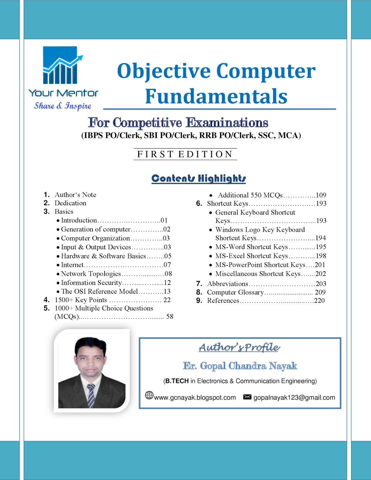
1. Author‘s Note
2. Dedication
3. Basics
- Introduction………………………........... 01
- Generation of computer………….............02
- Computer Organization……………..........03
- Input & Output Devices……….…............03
- Hardware & Software Basics……….........05
- Internet……………............…...............…07
- Network Topologies………………….......08
- Information Security…………………......12
- The OSI Reference Model……………….13
5. 1000+ Multiple Choice Questions (MCQs).... 58
- Additional 550 MCQs.........................…..109
- General Keyboard Shortcut Keys……………………………………….....….193
- Windows Logo Key Keyboard Shortcut Keys……………………………......194
- MS-Word Shortcut Keys…………………………………………………...…195
- MS-Excel Shortcut Keys……………………………………………………...198
- MS-PowerPoint Shortcut Keys…………………………………………..…...201
- Miscellaneous Shortcut Keys ………………………………………………...202
8. Computer Glossary…………………………………………………....….......…. 209
9. References……………………………………………………………….........….220
 |
| TO DOWNLOAD |
Aptitude Skill Test-Target IBPS Series by Er. G.C Nayak


Contents Highlights
Contains 105 selected word problems with answer key covering all important sections of Quantitative Aptitude. Every question is based on a unique Concept. Use the quickest approach to solve the questions.
|
| TO DOWNLOAD |
Voltage Multiplier
A voltage multiplier is an
electrical circuit that converts AC electrical power from a lower voltage to a
higher DC voltage, typically using a network of capacitors and diodes.
Voltage multipliers can be
used to generate a few volts for electronic appliances, to millions of volts
for purposes such as high-energy physics experiments and lightning safety
testing. The most common type of voltage multiplier is the half-wave series
multiplier, also called the Villard cascade.
 |
| Villard Cascade Voltage Multiplier |
Operation:
Assuming
that the peak voltage of the AC source is +Us, and that the C values are
sufficiently high to allow, when charged, that a current flows with no
significant change in voltage, then the (simplified) working of the cascade is
as follows:

Steps:
Ø negative
peak (−Us): The C1 capacitor is charged through diode D1 to Us V (potential
difference between left and right plate of the capacitor is Us)
Ø positive
peak (+Us): the potential of C1 adds with that of the source, thus charging C2
to 2Us through D2
Ø negative
peak: potential of C1 drops to 0 V thus allowing C3 to be charged through D3 to
2Us.
Ø positive
peak: potential of C1 rises to 2Us (analogously to step 2), also charging C4 to
2Us. The output voltage (the sum of voltages under C2 and C4) raises till 4Us.
In
reality more cycles are required for C4 to reach the full voltage. Each
additional stage of two diodes and two capacitors increases the output voltage
by twice the peak AC supply voltage.
Voltage
Doubler & Tripler:

A voltage doubler uses two
stages to approximately double the DC voltage that would have been obtained
from a single-stage rectifier. An example of a voltage doubler is found in the
input stage of switch mode power supplies containing a SPDT switch to select
either 120 volt or 240 volt supply. In the 120 volt position the input is
typically configured as a full-wave voltage doubler by opening one AC
connection point of a bridge rectfier, and connecting the input to the junction
of two series-connected filter capacitors. For 240 volt operation, the switch
configures the system as a full-wave bridge, re-connecting the capacitor center-tap
wire to the open AC terminal of a bridge rectfier system. This allows 120 or
240 volt operation with the addition of a simple SPDT switch.

A voltage tripler is a
three-stage voltage multiplier. A tripler is a popular type of voltage
multiplier. The output voltage of a tripler is in practice below three times
the peak input voltage due to their high impedance, caused in part by the fact
that as each capacitor in the chain supplies power to the next, it partially
discharges, losing voltage doing so.
Triplers were commonly used in
color television receivers to provide the high voltage for the cathode ray tube
(picture tube). Many 1970s TV sets used open triplers, and the individual diode
sticks could be replaced if they failed

Applications:
- In TV & Cathode Ray Tubes For High Voltage Supply
- In Xerox Machines To Produce High Voltage
- In High Energy Physics Cockcroft–Walton generator
Zener Diode As Regulator
 |
| Zener Diode |
We
know that "reverse biased" diode blocks current in the reverse
direction, but will suffer from premature breakdown or damage if the reverse
voltage applied across it is too high. However, the Zener Diode or "Breakdown
Diode" as they are sometimes called, are basically the same as the
standard PN junction diode but are specially designed to have a low
pre-determined Reverse Breakdown Voltage that takes advantage
of this high reverse voltage. The zener diode is the simplest types
of voltage regulator and the point at which a zener diode breaks down or
conducts is called the "Zener Breakdown Voltage" ( Vz ).
Doping
concentration of P+N DIODE > ZENER DIODE > TUNNEL DIODE>
PN DIODE
The Zener diode when biased in the
forward direction it behaves just like a normal signal diode passing the rated
current, but as soon as a reverse voltage applied across the zener diode
exceeds the rated voltage of the device, the diodes breakdown voltage VB is
reached at which point a process called Avalanche Breakdown occurs
in the semiconductor depletion layer and a current starts to flow through the
diode to limit this increase in voltage.
The current now flowing through the zener diode increases
dramatically to the maximum circuit value (which is usually limited by a series
resistor) and once achieved this reverse saturation current remains fairly
constant over a wide range of applied voltages. This breakdown voltage point, Vz is called the
"zener voltage" for zener diodes and can range from less than one
volt to hundreds of volts.
Zener
Diode I-V Characteristics:
The Zener Diode is used in its "reverse bias" or reverse breakdown mode, i.e. the diodes anode connects to the negative supply. From the I-V characteristics curve above, we can see that the zener diode has a region in its reverse bias characteristics of almost a constant negative voltage regardless of the value of the current flowing through the diode and remains nearly constant even with large changes in current as long as the zener diodes current remains between the breakdown current IZ(min) and the maximum current rating IZ(max).

The Zener Diode As Regulator:
Zener Diode Acts as a Voltage Regulator only in the Reverse
Breakdown Region.A voltage regulator should maintain constant voltage across terminals of
load irrespective of fluctuation in Load or Supply.To act as a voltage
regulator the zener diode must satisfy two conditions:
(i) Current through zener diode should be grater than or
equal to IZ(min),knee current.
(ii)Voltage across terminals of
zener diode should be Vz, Breakdown voltage.

The resistor, RS is connected in series with the zener diode to limit the current flow through the diode with the voltage source, VS being connected across the combination. The stabilised output voltage Vout is taken from across the zener diode. The zener diode is connected with its cathode terminal connected to the positive rail of the DC supply so it is reverse biased and will be operating in its breakdown condition. Resistor RS is selected so to limit the maximum current flowing in the circuit.
With
no load connected to the circuit, the load current will be zero, ( IL = 0 ),
and all the circuit current passes through the zener diode which in turn
dissipates its maximum power. Also a small value of the series resistor RS will
result in a greater diode current when the load resistance RL is
connected and large as this will increase the power dissipation requirement of
the diode so care must be taken when selecting the appropriate value of series
resistance so that the zeners maximum power rating is not exceeded under this
no-load or high-impedance condition.
The
load is connected in parallel with the zener diode, so the voltage across RL is
always the same as the zener voltage, ( VR = VZ ).
There is a minimum zener current for which the stabilization of the voltage is
effective and the zener current must stay above this value operating under load
within its breakdown region at all times. The upper limit of current is of
course dependant upon the power rating of the device. The supply voltage VS must
be greater than VZ.
One
small problem with zener diode stabiliser circuits is that the diode can
sometimes generate electrical noise on top of the DC supply as it tries to
stabilise the voltage. Normally this is not a problem for most applications but
the addition of a large value decoupling capacitor across the zeners output may
be required to give additional smoothing.
Then
to summarise a little. A zener diode is always operated in its reverse biased
condition. A voltage regulator circuit can be designed using a zener diode to
maintain a constant DC output voltage across the load in spite of variations in
the input voltage or changes in the load current. The zener voltage regulator
consists of a current limiting resistor RS connected in series
with the input voltage VS with the zener diode
connected in parallel with the load RL in this reverse
biased condition. The stabilized output voltage is always selected to be the
same as the breakdown voltage VZ of the diode.
Zener Diode Voltages
As well as producing a single stabilised voltage output,
zener diodes can also be connected together in series along with normal silicon
signal diodes to produce a variety of different reference voltage output values
as shown below.
Zener Diodes
Connected in Series:

The
values of the individual Zener diodes can be chosen to suit the application
while the silicon diode will always drop about 0.6 to 0.7V in the forward bias
condition. The supply voltage, Vin must
of course be higher than the largest output reference voltage and in our
example above this is 19v.
Zener Diode Clipping Circuits:
Thus
far we have looked at how a zener diode can be used to regulate a constant DC
source but what if the input signal was not steady state DC but an alternating
AC waveform how would the zener diode react to a constantly changing signal.
Diode
clipping and clamping circuits are circuits that are used to shape or modify an
input AC waveform (or any sinusoid) producing a differently shape output
waveform depending on the circuit arrangement. Diode clipper circuits are also
called limiters because they limit or clip-off the positive (or negative) part
of an input AC signal. As zener clipper circuits limit or cut-off part of the
waveform across them, they are mainly used for circuit protection or in
waveform shaping circuits.
For
example, if we wanted to clip an output waveform at +7.5V, we would use a 7.5V
zener diode. If the output waveform tries to exceed the 7.5V limit, the zener
diode will "clip-off" the excess voltage from the input producing a
waveform with a flat top still keeping the output constant at +7.5V. Note that
in the forward bias condition a zener diode is still a diode and when the AC
waveform output goes negative below -0.7V, the zener diode turns "ON"
like any normal silicon diode would and clips the output at -0.7V as shown
below.
Square Wave Signal:

The
back to back connected zener diodes can be used as an AC regulator producing
what is jokingly called a "poor man's square wave generator". Using
this arrangement we can clip the waveform between a positive value of +8.2V and
a negative value of -8.2V for a 7.5V zener diode. If we wanted to clip an
output waveform between different minimum and maximum values for example, +8V
and -6V, use would simply use two differently rated zener diodes.
Note
that the output will actually clip the AC waveform between +8.7V and -6.7V due
to the addition of the forward biasing diode voltage, which adds another 0.7V
voltage drop to it. This type of clipper configuration is fairly common for
protecting an electronic circuit from over voltage. The two zeners are
generally placed across the power supply input terminals and during normal
operation, one of the zener diodes is "OFF" and the diodes have
little or no affect. However, if the input voltage waveform exceeds its limit,
then the zeners turn "ON" and clip the input to protect the circuit.
Superheterodyne Receiver
In electronics, a
superheterodyne receiver (often shortened to superhet) uses frequency mixing or
heterodyning to convert a received signal to a fixed intermediate frequency
(IF), which can be more conveniently processed than the original radio carrier
frequency. Virtually all modern radio receivers use the superheterodyne principle.


Block
diagram:

The
diagram contains a RF amplifier, a variable frequency local oscillator(LO), a
frequency mixer, a band pass filter and intermediate frequency (IF) amplifier,
and a demodulator plus additional circuitry to amplify or process the original
audio signal (or other transmitted information).For AM The Intermediate
frequency(IF) is 455Hz.
principle
of operation:
The
principle of operation of the superheterodyne receiver depends on the use of
heterodyning or frequency mixing. The signal from the antennal i.e RF Signal (fs)
is filtered sufficiently at least to reject the image frequency (see below) and possibly amplified by RF Amplifier.
A local oscillator(LO) in the receiver produces a sine wave( i.e fl ) which mixes with that
signal, shifting it to a specific intermediate frequency (IF= fl – fs OR fIF = fLO - fRF),
usually a lower frequency(i.e Mixer
performs Down Conversion Here).The IF signal is itself filtered and
amplified and possibly processed in additional ways. The demodulator uses the
IF signal rather than the original radio frequency to recreate a copy of the
original information (such as audio).An AF amplifier used to amplify audio
signal.
Image
Frequency & its suppression:
One
major disadvantage to the superheterodyne receiver is the problem of image
frequency. In heterodyne receivers, an image frequency is an undesired input
frequency equal to the station frequency plus twice the intermediate frequency.
The image frequency results in two stations being received at the same time,
thus producing interference. Image frequencies can be eliminated by sufficient
attenuation on the incoming signal by the RF amplifier filter of the
superheterodyne receiver.
fimg(Image Frequency) = fs +2* fIF
For
example, an AM broadcast station at 580 kHz is tuned on a receiver with a 455
kHz IF. The local oscillator is tuned to 580 + 455 = 1035 kHz. But a signal at
580 + 455 + 455 = 1490 kHz is also 455 kHz away from the local oscillator; so
both the desired signal and the image, when mixed with the local oscillator,
will also appear at the intermediate frequency. This image frequency is within
the AM broadcast band.
Practical
receivers have a tuning stage before
the converter, to greatly reduce the amplitude of image frequency signals;
additionally, broadcasting stations in the same area have their frequencies
assigned to avoid such images.

Image
Rejection Ratio:
To
determine the suppression factor of tuned ckt image rejection ratio is used.
The
image rejection ratio, or image frequency rejection ratio, is the ratio of the
intermediate-frequency (IF) signal level produced by the desired input
frequency to that produced by the image frequency. The image rejection ratio is
usually expressed in db.
Mathematically,

where Q=Quality factor, fimg=Image frequency, fs=RF Signal frequency
Note
that IMRR is not a measurement of the performance of the IF stages or IF
filtering (selectivity); the signal yields a perfectly valid IF frequency.
Rather, it is the measure of the bandpass characteristics of the stages
preceding the IF amplifier, which will consist of RF bandpass filters and
usually an RF amplifier stage or two.
NOTE: The
image frequency should be suppressed before the mixer stage.Practically IRR
Should be as high as possible ,so the tuned circuits are connected in cascade.if X is the IRR Of tuned ckt 1
&Y is the IRR of tuned ckt 2
then IRR of the cascaded stage is X*Y.To improve the IRR either Q Factor or IF should be
increased but to increase IRR we practically prefer to increase IF Because
increasing Q Factor causes decrease in Bandwidth.
Subscribe to:
Posts (Atom)